


The digital landscape is evolving at an unprecedented pace. From smartphones and wearables to autonomous vehicles and hyperscale data centers, the demand for faster, smarter, and more efficient electronics is reshaping the semiconductor industry. At the core of this transformation is heterogeneous integration—the convergence of multiple technologies, functions, and components into unified systems through advanced packaging.
This shift is not just about miniaturization or performance gains. It’s about enabling entirely new capabilities across industries, unlocking the full potential of artificial intelligence (AI), 5G, edge computing, and beyond.
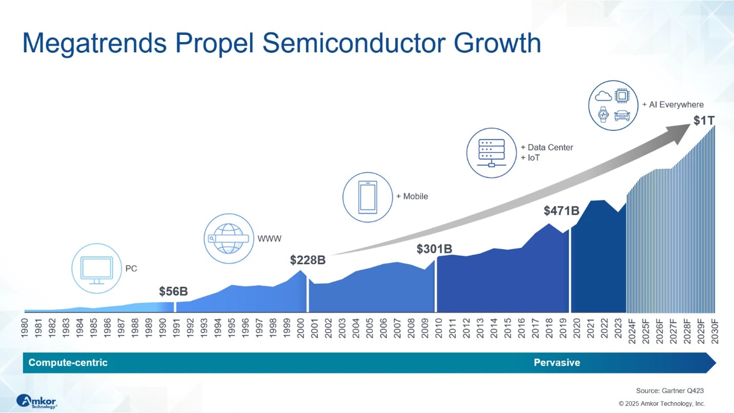
The semiconductor supercycle: Driven by megatrends
The semiconductor market is on a trajectory to exceed $1 trillion in the coming years, propelled by several converging megatrends:
- AI Everywhere: From generative models in data centers to personalized assistants on mobile devices.
- 5G and Next-Gen Connectivity: Enabling ultra-low latency and massive data throughput.
- Automotive Digitization: Software-defined vehicles (SDVs) and autonomous systems are redefining mobility.
- Edge Computing: Real-time data processing at the device level for faster decision-making.
These trends are creating a need for high-performance, energy-efficient, and scalable packaging solutions that can support increasingly complex workloads.

Advanced packaging: The engine for innovation
Traditional monolithic chip designs are reaching their limits. Advanced packaging offers a new path forward by enabling:
- 2.5D and 3D Integration: Stacking dies vertically using interposers and through-silicon vias (TSVs).
- Chiplet Architectures: Modular design that improves yield, reduces cost, and accelerates time-to-market.
- Fan-Out Wafer-Level Packaging (WLFO): High-density, low-profile solutions for mobile and wearable devices.
- Co-Packaged Optics (CPO): Integrating photonics directly into the package for ultra-fast data transmission.
These technologies allow for the integration of logic, memory, RF, and photonics in compact, high-performance systems—essential for modern AI, communications, and compute applications.

AI deployment: Cloud vs. edge
AI is no longer confined to massive data centers. It’s increasingly being deployed at the edge—in smartphones, vehicles, and IoT devices. This shift introduces two distinct paradigms:
| Feature | Cloud-Based AI | On-Device AI |
| Connectivity | High | Local |
| Latency | High | Low |
| Hardware | Centralized | Decentralized |
| Model Size | Large (LLM) | Small/Medium (SLM) |
| Personalization | Limited | High |
Advanced packaging enables both by integrating compute, memory, and interconnects in ways that optimize performance, power efficiency, and form factor.
Automotive transformation: The rise of SDVs
The automotive industry is undergoing a seismic shift. Vehicles are becoming intelligent platforms, powered by domain-based architectures and AI-driven features such as:
- Augmented reality displays
- Predictive maintenance
- Collision avoidance and ADAS
- In-vehicle inferencing and edge AI
Compute content per vehicle is expected to exceed $1000 by 2030, driven by the integration of high-performance processors, memory, sensors, and RF modules. Packaging innovations like leadframe evolution, multi-chip modules (MCMs), and system-in-package (SiP) are critical to meeting these demands.

Technology toolboxes: Building blocks of the future
To support this complexity, a robust set of packaging technologies is required:
- Interposers: Silicon, RDL, and glass for signal routing and power delivery
- Bonding Techniques: Mass reflow, thermocompression, and laser-assisted bonding
- Substrates: Coreless, thin-core, and organic damascene for improved thermal and electrical performance
- Thermal Management: Advanced TIMs, direct liquid cooling, and backside metallization
- Embedded Passives: Capacitors and resistors integrated into the package for space savings and performance
These toolboxes enable scalable, reliable, and high-performance systems across mobile, automotive, and data center applications.
Global manufacturing at scale
Meeting the demands of next-generation electronics requires more than just innovation, it requires scale, speed, and resilience. Advanced packaging technologies are complex and require precision manufacturing, robust supply chains, and global coordination.
Amkor’s global footprint is a key differentiator in this landscape. With over 12 million square feet of manufacturing space across strategic locations in Asia, Europe, and soon in the United States, Amkor offers customers unmatched flexibility and reliability. This extensive network enables:
- Regional manufacturing options to support localized supply chains
- Scalable capacity for high-volume production
- Redundancy and risk mitigation across geographies
- Faster time-to-market through proximity to design and assembly hubs
By combining advanced technology capabilities with a broad geographic presence, Amkor delivers a comprehensive supply chain offering, empowering customers to innovate confidently and compete globally.
Design and test: A new paradigm
Advanced packaging demands a rethinking of design and test methodologies:
- Co-Design and Co-Optimization: Integrating IC and package design for better performance and reliability
- Standardization: Emerging standards like UCIe are addressing interoperability and testability in multi-chiplet systems
- Smart Design Kits: Streamlining the design-to-manufacturing pipeline with integrated rule sets and simulation tools
Testing is also evolving, with new methods required to validate individual dies, interconnects, and stacked topologies in increasingly complex packages.
Conclusion: Integration is innovation
Heterogeneous integration is more than a technical milestone—it’s a strategic enabler of the next wave of digital transformation. As devices become smarter and systems more interconnected, advanced packaging will be the key to unlocking performance, efficiency, and innovation across the data spectrum.
From enabling AI on your smartphone to powering autonomous vehicles and hyperscale data centers, advanced packaging is the invisible force driving the future of electronics.
Ready to accelerate your innovation?
Whether you’re designing next-gen mobile devices, building AI-enabled automotive platforms, or scaling data center infrastructure, advanced packaging is the key to unlocking performance and efficiency.
Partner with Amkor to leverage our global manufacturing footprint, cutting-edge technology toolboxes, and decades of packaging expertise. Let’s build the future—together. Contact us to explore how our solutions can support your next breakthrough.
The post Enabling The Future: Heterogeneous Integration From Connected Devices To Data Centers appeared first on Semiconductor Engineering.