

The semiconductor industry faces an unprecedented paradox: AI demand is booming, fab investments are rising, yet wafer shipments remain stubbornly flat. What’s driving this disconnect, and when will it break?
As of mid-2025, the global silicon wafer market appears calm on the surface, but underlying structural tensions are quietly mounting. The demand for AI semiconductors remains resilient, and certain high-value supply chains continue to operate near capacity. Yet wafer shipments have shown little sign of meaningful recovery—a divergence that raises questions about the conventional supply-demand playbook.
SEMI’s latest Silicon Wafer Market Monitor Report begins with a structural hypothesis: that the current market dynamics cannot be explained solely by weak demand or delayed orders. Instead, we propose that the demand pattern of fab operations itself has fundamentally changed.
The hidden constraint: Time extension
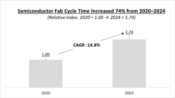
One critical metric has emerged as a structural bottleneck—fab cycle time, or the average duration for a wafer to complete its full process flow. Our quantitative analysis reveals that since 2020, fab cycle times have grown at a compound annual growth rate of 14.8%. This represents a fundamental deceleration in fab throughput, meaning that even with the same number of tools and consistent utilization rates, the volume of wafers that can be processed is now structurally constrained.
Why is this happening? Rising process complexity, increased equipment density, and tighter quality control requirements are absorbing more capital per wafer while paradoxically slowing production. Equipment spending per wafer area has surged over 150% since 2020, yet this investment translates into longer processing times rather than higher throughput.
The High Bandwidth Memory (HBM) economic threshold
Simultaneously, the market is approaching a new inflection point driven by the rapid rise of HBM. HBM wafers consume over three times more wafer area per bit compared to standard DRAM, creating potentially significant wafer demand. However, HBM currently accounts for just 16% of total memory revenue—still below a critical economic threshold.
Our analysis identifies that when HBM reaches 25% of total memory revenue, the trade ratio rises to 1.5. This is the structural breakeven point where CapEx per wafer for HBM-dedicated lines aligns with standard DRAM economics. At this threshold, memory makers gain clear incentives to expand wafer input, and customers become more willing to pay premium prices.
The quantitative framework
Instead of relying on conventional forecasts, we model the interaction of four critical variables—HBM penetration, DRAM bit growth, fab utilization, and cycle time—using a quantitative simulation framework. Under current conditions (16% HBM revenue share, 15% annual bit growth, 95% fab utilization, and 14.8% cycle time increase), wafer input would need to increase by 23.9% annually to meet projected demand.
Yet no fab is scaling wafer input to that extent today. This suggests the market isn’t demand-constrained but operating within a conditionally responsive system—one that won’t activate until key thresholds align.
Beyond economics: Technical and operational readiness
The slow pace of HBM expansion isn’t solely about investment timing. Technical constraints, including low yields, delayed customer qualification, and process stabilization challenges, also play critical roles. These preconditions—investment readiness, yield optimization, and qualification completion—haven’t yet aligned, keeping the market in strategic latency despite robust underlying demand.
Additional factors compound this delay. Backend bottlenecks in Chip-on-Wafer-on-Substrate (CoWoS) packaging are causing semi-finished wafers to accumulate as inventory, constraining upstream wafer input. At the fab level, companies prioritize efficiency gains through process conversions over new construction. Meanwhile, macroeconomic uncertainty, geopolitical tensions, and foreign exchange volatility continue suppressing capital execution.
The three-tier response model
This structural shift creates a three-tier demand response across the supply chain:
- Wafer demand: Conditionally responsive, awaiting economic threshold alignment
- Equipment investment: Process-transition driven, already responding to complexity increases
- Materials demand: Directly tied to cycle time extensions, with potential for early bottlenecks
For certain process-critical materials like EUV photoresists and TSV chemicals, supply constraints may emerge even before wafer input fully ramps, preceding equipment expansion.
Strategic implications
For industry stakeholders, this analysis suggests three key actions: wafer suppliers should prepare scenario-based capacity plans around the 25% HBM threshold; equipment makers should anticipate process-transition driven demand regardless of current wafer volumes; and materials suppliers should prepare for potential bottlenecks as extended cycle times increase consumption per wafer.
Crucially, the current stagnation shouldn’t be interpreted as structural decline. Rather, the market exists in a state of strategic readiness, with key conditions not yet aligned. Once they are, wafer demand will likely respond nonlinearly—and momentum is already building in that direction.
The structural inflection point (≈25% HBM penetration) and cycle time increase (+14.8%) serve as forward-looking indicators not just for wafer producers, but for the entire upstream supply chain. The question isn’t whether this inflection will occur, but when. Companies that understand these structural dynamics and prepare accordingly will be best positioned to capitalize on the nonlinear demand response when it arrives.
These key insights are from the market update section of the Q2 2025 Silicon Wafer Market Monitor Report. This quarter’s analysis models structural inflection points using scenario-based projections across nine core charts and tables, offering data-driven perspective on the industry’s readiness for the next demand shift. Download your free sample report today.
The post From Latency To Reaction: Simulating The Next Wafer Demand Inflection appeared first on Semiconductor Engineering.